- Home
- Braemac Blog
- From Silicon Labs: "Timing 101 #10: The Case of the Half-terminated Differential Output Clock"
From Silicon Labs: "Timing 101 #10: The Case of the Half-terminated Differential Output Clock"

About Symmetry Electronics
Established in 1998, Symmetry Electronics, a Division of Braemac, is a global distributor of electronic components and systems. Combining premier components and comprehensive value-added services with an expert in-house engineering team, Symmetry supports engineers in the design, development, and deployment of a broad range of connected technologies.
Exponential Technology Group Member
Acquired by Berkshire Hathaway company TTI, Inc. in 2017, Symmetry Electronics is a proud Exponential Technology Group (XTG) member. A collection of specialty semiconductor distributors and engineering design firms, XTG stands alongside industry leaders TTI Inc., Mouser Electronics, and Sager Electronics. Together, we provide a united global supply chain solution with the shared mission of simplifying engineering, offering affordable technologies, and assisting engineers in accelerating time to market. For more information about XTG, visit www.xponentialgroup.com.
Introduction
In this month’s post, I will review a basic, but sometimes overlooked, best practice necessary for making proper output clock measurements.
Those of you familiar with our clock IC evaluation boards know that we generally AC-couple our input and output clocks and provide separate SMA RF connectors for each polarity of the differential clock signal. This is the most flexible approach in terms of being able to immediately connect output clocks to single-ended 50 Ω inputs on test equipment such as frequency counters, oscilloscopes, phase noise analyzers, spectrum analyzers, etc. The AC-coupling capacitors keep us from attempting to impose a DC bias on test equipment inputs and vice-versa.
Here’s the best practice rule: Both polarities of differential output buffers should be terminated when making measurements. This include the polarity that is not being measured. What are the consequences for not doing this? That is the subject of this article, The Case of the Half-terminated Differential Output Clock.
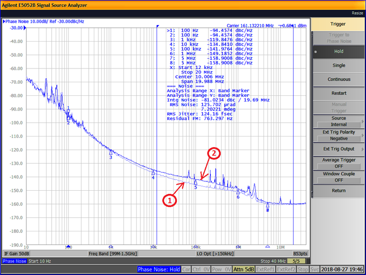
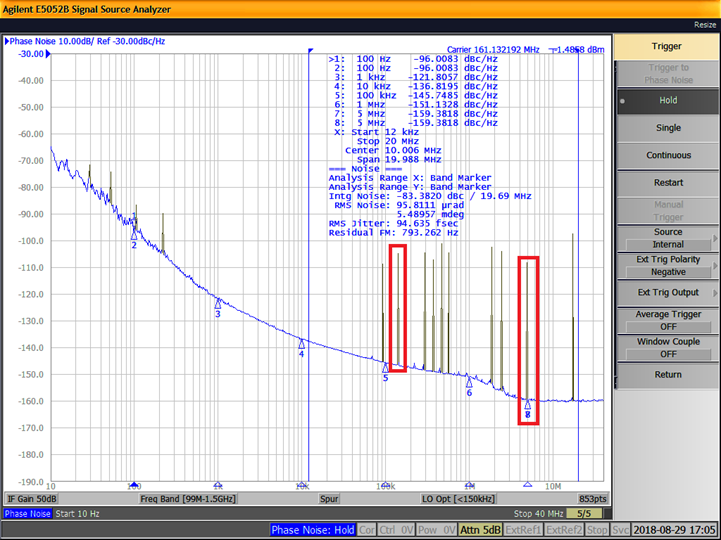
Example Phase Noise Measurement
First, let’s work in the frequency domain. Consider the phase noise plot below. It is from OUT0 of an Si5345 evaluation board for these 2 cases annotated in the screen capture.
- OUT0B is routed to a 50 Ω oscilloscope input. This is the properly (fully) terminated case.
- OUT0B is routed to a 1 MΩ oscilloscope input. This is the half-terminated case.
The output format is 2.5V LVDS AC-coupled with the nominal frequency set to 161.1328125 MHz based on the current CBPro sample plan. The board is actually in Free Run mode just to minimize the bench set-up.
In the first case, the 12 kHz to 20 MHz RMS phase jitter measured 89.512 fs. This curve was saved in memory. In the second case, the 12 kHz to 20 MHz RMS phase jitter increased to 124.16 fs. That’s not bad but the relative increase is about 39%. That is a significant impact.
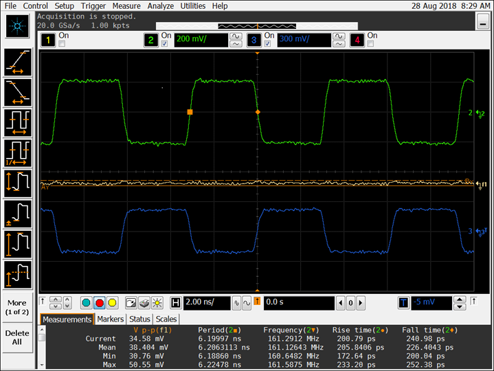
Example Oscilloscope Measurements
Next we’ll work in the time domain. Consider the oscilloscope plots below. The top trace is OUT0 assigned to channel 2, OUT0B is assigned to channel 3, and the common mode (CM) voltage is computed as f1. Note that since we are on the far side of the AC-coupling capacitor, we aren’t measuring the DC value but rather the noise represented by the average value of AC-coupled OUT0 and OUT0B. (The difference in scales here is to accommodate the half-terminated case and is not relevant to the calculation.)
In this first screen capture, both oscilloscope inputs are set to 50 Ω. The waveform shapes look reasonable and the CM noise is about 38mVpp on average.
In this second screen capture, the only difference is that OUT0B’s input has been set to 1 MΩ. Now both waveform shapes are larger and distorted. Further, the CM noise has increased to about 344 mVpp on average. This is almost an order of magnitude increase in CM noise.
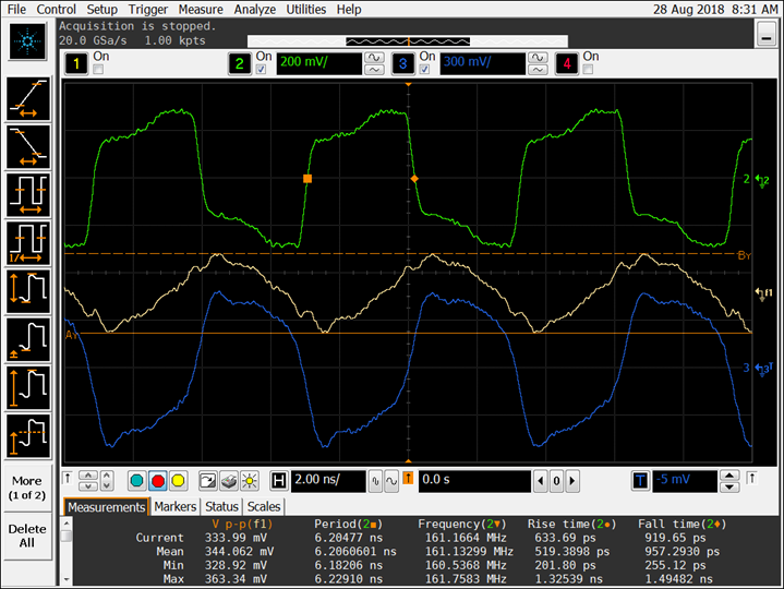
Note that in these experiments, the time domain measurements are much more striking than the frequency domain measurements. The phase noise differences might even have been glossed over in automated testing. A good argument for a lab bench to have both types of instrumentation!
Root Cause
Why is terminating only half of the output clock having such an impact? We don’t need to know all the details of the buffer’s design but a simplified model will provide some insight. Consider the figure below.

Components in the left hand side box are internal to the IC and illustrate a simplified model of a CML or Current Mode Logic driver that can be made compatible with several swing formats. The AC-coupling caps are usually on the EVB and the load resistor R shown here is typically 50 Ω as for test equipment. Transmission lines are not illustrated but PCB traces and coaxial cable can all be assumed to be nominal 50 Ω. (The AC coupled load terminations can also be regarded as 100 Ω differential across CLKP and CLKN where the center-tap CM voltage is GND.)
Some notable features include the following:
- Current source Ibias sinks continuously. To first order, current is switched through one of the input NMOS transistors when turned fully on depending on the input signals.
- The internal termination resistors Rint are normally ~ R or perhaps 2*R to save current.
- Common mode voltage Vcm is sensed at the center-point of 2 resistors Rcm. The value of these resistors is usually >> R, for example on the order of kΩ.
- An op amp drives the Bias network so that the sensed Vcm is equal to Vref.
- Each output voltage swing is based on Vsupply minus the voltage drop swing across Rint as the current changes.
The driver is symmetric and designed for specific DC biasing over expected terminated operation. DC-coupled loads would need to have a common voltage exactly equal to Vcm in order to not impact the intended bias. This is why we need to AC-couple to instrument loads.
However, even if we are AC-coupled, if we don’t have symmetric loads, then the driver will be imbalanced and the result is that the output common mode voltage Vcm will be modulated which can impact biasing and operation. In this particular case the CM feedback circuit is clearly unable to keep up. The performance of the measured terminated half-circuit is degraded by the operation of the unterminated half-circuit.
Crosstalk
Half-terminated differential outputs can even impact neighboring output driver performance in subtle ways. In this experiment, we continue to work with an Si5345 EVB as before. The phase noise plot below is for OUT0 set to nominal 161.1328125 MHz as before with OUT0B terminated. Adjacent channel OUT1/OUT1B is set to nominal 2 times that or 322.265625 MHz. Both polarities are properly terminated. The 12 kHz to 20 MHz phase jitter measured 94.32 fs averaged over 5 sweeps. Spurs are depicted in dBc so we can see the details.
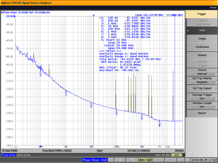
The next phase noise plot is for OUT0 again, under previous conditions, except this time neighboring output OUT1B is unterminated. There is not a significant increase in phase jitter. However, we have clearly introduced 2 new spurs above the powerline frequencies region as annotated below.
These were identified in the instrument spur list as 140.374 kHz at -104.874 dBc and 4.90 MHz at -108.235 dBc. There is no obvious mathematical relationship yet this is a consistent result for this board and configuration. For wireless applications interested in the reason for every spur we can at least attribute these to the adjacent channel’s improper termination.
Termination Options
There are a number of termination options for our evaluation boards, and similar application boards, depending on what’s available at your bench. These include:
- Use a differential limiting amplifier or balun to convert a differential clock in to a single-ended clock.
- Connect each polarity in to a 50 Ω instrument input.
- Terminate each unmeasured polarity using an SMA 50 RF load termination.
If one is attempting to make careful measurements on a 12 output evaluation board that could call for 24 – 1 or 23 SMA terminations. That’s a fair number. So what to do?
One approach is to just make sure that the nearest channel output clocks to the measured clock are terminated. That cuts the quantity down quite a lot. The other is to use RF pads or attenuators as described in the next section.
Attenuators as Lab Expedient Terminations
In our lab we have many multi-channel clock EVBs which can consume a large quantity of terminations during testing. If a lot of us are working in the lab simultaneously, we can’t always terminate every clock exactly the way we would like. So another approach is to use a high value RF pad or attenuator as a lab expedient termination.
Commercially available attenuators are PI attenuators made up of a 3-resistor network. That is, the resistor network resembles the Greek letter "pi". The first resistor R1 is shunted to GND, followed by R2 in series, followed by another R1 shunted to GND.
Using an online calculator such as at https://www.microwaves101.com/calculators/858-attenuator-calculator we can calculate the R1 and R2 values and the resulting effective Rload assuming no connection past the attenuator. The table below lists the effective load using 6 dB, 10 dB, and 20 dB terminations.
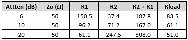
You can see that for increasing attenuator values the effective impedance looking in to the attenuator alone increases. By 20 dB attenuation it’s an almost perfect termination. This can be very handy at times. The results using this technique are indistinguishable from purpose-built terminations.
Conclusion
I hope you have enjoyed this Timing 101 article. I’ve given you some insight as to why it’s a best practice to terminate even unmeasured differential outputs. And provided a tip for using an attenuator as a lab expedient termination if necessary.
As always, if you have topic suggestions, or there are questions you would like answered, appropriate for this blog, please send them to kevin.smith@silabs.com with the words Timing 101 in the subject line. I will give them consideration and see if I can fit them in. Thanks for reading. Keep calm and clock on.
Cheers,
Kevin
Source: https://www.silabs.com/community/blog.entry.html/2018/08/31/timing_101_10_the-NGZP
Looking to integrate Silicon Labs products with your design? Our Applications Engineers offer free design and technical help for your latest designs. Contact us today!
About Symmetry Electronics
Established in 1998, Symmetry Electronics, a Division of Braemac, is a global distributor of electronic components and systems. Combining premier components and comprehensive value-added services with an expert in-house engineering team, Symmetry supports engineers in the design, development, and deployment of a broad range of connected technologies.
Exponential Technology Group Member
Acquired by Berkshire Hathaway company TTI, Inc. in 2017, Symmetry Electronics is a proud Exponential Technology Group (XTG) member. A collection of specialty semiconductor distributors and engineering design firms, XTG stands alongside industry leaders TTI Inc., Mouser Electronics, and Sager Electronics. Together, we provide a united global supply chain solution with the shared mission of simplifying engineering, offering affordable technologies, and assisting engineers in accelerating time to market. For more information about XTG, visit www.xponentialgroup.com.