- Home
- Braemac Blog
- From Silicon Labs: "Timing 101 #11: The Case of the Noisy Source Clock Tree Part 1"
From Silicon Labs: "Timing 101 #11: The Case of the Noisy Source Clock Tree Part 1"
About Symmetry Electronics
Established in 1998, Symmetry Electronics, a Division of Braemac, is a global distributor of electronic components and systems. Combining premier components and comprehensive value-added services with an expert in-house engineering team, Symmetry supports engineers in the design, development, and deployment of a broad range of connected technologies.
Exponential Technology Group Member
Acquired by Berkshire Hathaway company TTI, Inc. in 2017, Symmetry Electronics is a proud Exponential Technology Group (XTG) member. A collection of specialty semiconductor distributors and engineering design firms, XTG stands alongside industry leaders TTI Inc., Mouser Electronics, and Sager Electronics. Together, we provide a united global supply chain solution with the shared mission of simplifying engineering, offering affordable technologies, and assisting engineers in accelerating time to market. For more information about XTG, visit www.xponentialgroup.com.
Introduction
In this post, The Case of the Noisy Source Clock Tree Part 1, we will go a step beyond the prototypical or “canonical” clock tree. I will discuss the motivation for adding a jitter attenuator and its impact on clock tree jitter estimation. So let’s get started.
The Canonical Clock Tree
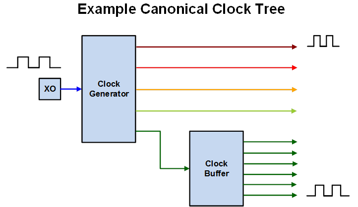
The board level clock tree or clock distribution network, for say a data center application, is typically depicted with a crystal or low jitter XO (crystal oscillator) connected to a clock generator followed by one or more buffers, something like the following. This is what I refer to as the canonical clock tree:

The root or source of the clock tree in this example is a low jitter XO which determines the frequency stability of the clock tree overall. The clock generator then scales the input frequency from the XO to several different (usually higher) output frequencies. Finally, the clock buffer takes one of these output frequencies and yields multiple output clocks with the same frequency. The colored arrows in the figure are meant to suggest different clock frequencies.
We can estimate the total or end clock phase jitter of the canonical clock tree by applying the RSS or Root Sum of the Squares of the individual contributions. (This is the same summation in quadrature math used in cascaded statistical analysis of mechanical tolerances and other errors or uncertainties.)
For the example above, we can estimate the total RMS phase jitter as

Note that several prerequisites must hold true for this calculation to be valid:
- The phase jitter contributions should be uncorrelated.
- Each phase jitter contribution must be integrated over the same jitter bandwidth, e.g. 12 kHz to 20 MHz.
- Finally, every device in the clock tree is wideband with respect to the clocks involved.
Jitter Transfer versus Jitter Generation versus Additive Jitter
The last statement above means that the bandwidth of the clock generator is wide enough compared to the input clock phase noise that we need not consider the clock generator’s jitter transfer. You may recall that jitter transfer or jitter attenuation measures output clock jitter versus input clock jitter. This is often written as the Jitter Transfer Function or JTF. A PLL’s JTF acts as a low pass filter to input jitter and is a function of PLL bandwidth.
Jitter generation refers to the intrinsic jitter of a device. In the case of a clock generator, it is a measure of the output jitter when an ideal (no jitter) input clock is applied. A PLL-based clock device, even with a perfect input clock applied, still has PFD (Phase Frequency Detector) path noise and an intrinsic phase noise source, the VCO. Thus the need for a jitter generation term.
By contrast, clock buffers consisting only of amplifiers and perhaps dividers will always contribute additional noise to any input clock. Hence the use of the term additive jitter.
The Noisy Source Case
The example canonical clock tree above assumes a low noise clock as in a typical application. However not all clock trees have a low noise clock source.
What categorizes a source clock as relatively low or high noise? Let’s ignore the follow-on clock buffer for now and just compare the XO’s jitter generation versus the clock generator’s jitter generation. If they were exactly the same, the total jitter would increase by a factor of SQRT(2) or 41% which is substantial. If we choose the usual engineering convention of a 10% increase denoting significance, then we can back out that the XO’s phase jitter should be < 46% of the clock generator’s phase jitter. In other words, the source jitter must approach approximately half the clock generator’s jitter to significantly increase the output clock jitter.
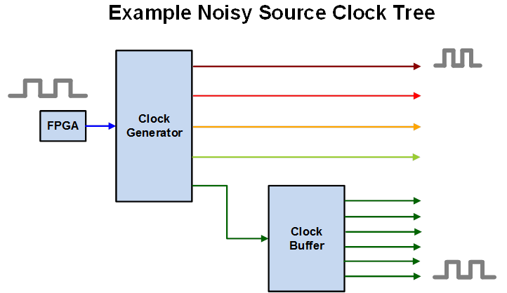
A noisy (jittery) clock could be a recovered clock from serial data or derived from an FPGA. Perhaps the board itself is introducing power supply noise in to the XO. Such a clock tree then behaves as indicated in the figure below. The waveforms are shown thicker here than in the previous figure to suggest higher jitter.

We can still apply the RSS estimate even for a noisy source clock. However, often the resulting jitter will be too high for a typical clock distribution application. So what is our recourse?
Jitter Attenuator to the Rescue
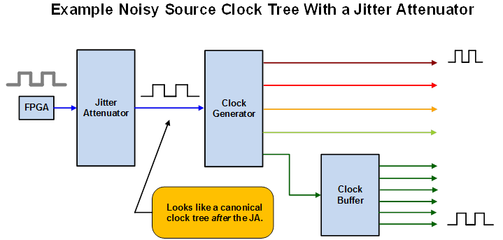
In such applications, we need to add a jitter attenuator to clean up the source clock noise and improve the clock tree jitter performance. The figure below illustrates the basic idea where we have inserted a jitter attenuator between the noisy FPGA-derived source clock and the clock generator. Post jitter attenuator, the rest of the clock tree now looks like the canonical case. Note that in practical applications, a single device often performs both the jitter attenuator and clock generator scaling functions.

Like the clock generator, the jitter attenuator is a PLL-based device whose JTF acts as a low pass filter to input jitter. However, unlike the clock generator, the jitter attenuator is a relatively narrow bandwidth device versus the input clock phase noise. This violates one of the prerequisites for using the RSS estimate method. So, what is the best approach to calculate the expected phase jitter of the jitter attenuator output clock, and by extension the total or end clock jitter?
Clock Tree as a Phase Noise Processing System
In engineering, we usually analyze and measure the performance of systems in the frequency domain. Clock distribution networks aka clock trees are no different. The primary attribute of a clock is its frequency and the RMS phase jitter quantities are integrated from phase noise data. It should come as no surprise then that the better and more rigorous way to analyze clock trees generally is in the frequency domain.
In fact, following the clock signal from the source through jitter attenuators, clock generators or multipliers, and buffers, to the sink or destination is best viewed as a system that processes phase noise (this is an example of “one man’s noise is another man’s signal”).
The application of jitter attenuators in particular can really only be well understood by working in the frequency domain. The JTF can be modeled simply by the PLL bandwidth and expected attenuation in the jitter bandwidth of interest. At each phase noise offset frequency f we calculate the output clock phase noise in terms of the input clock phase noise, shaped by the JTF, and added in quadrature to the jitter generation phase noise contribution. We can then check to see if the resulting integrated phase jitter meets the required jitter performance.
I will discuss in more detail exactly how to do this and provide a measurement and spreadsheet example in the next post, The Case of the Noisy Source Clock Tree Part 2.
Conclusion
I hope you have enjoyed this Timing 101 article and will look forward to the follow-up.
As always, if you have topic suggestions, or there are questions you would like answered, appropriate for this blog, please send them to kevin.smith@silabs.com with the words Timing 101 in the subject line. I will give them consideration and see if I can fit them in. Thanks for reading. Keep calm and clock on.
Cheers,
Kevin
Source: https://www.silabs.com/community/blog.entry.html/2018/10/30/timing_101_11_the-2uqO
